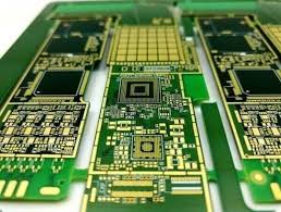
HDI Printed Circuit Boards
The HDI PCB (printed circuit board) allows for a higher number of interconnections in a smaller area. It also has improved electrical performance, which leads to smaller components and a reduction in power consumption. Additionally, the shorter distance between components means faster signal transmissions, resulting in lower crossing delays and EMI.
This technology is used in complex electronic devices that require superior performance while saving space. These include mobile/cellular phones, touch screen devices, laptop computers, digital cameras and 4/5G network communications, as well as military applications such as smart munitions.
Advanced medical equipment also relies on HDI circuit boards for better functionality and reliability. Whether it’s monitoring, scanning, X-ray or lab tests, these devices must be functional and accurate to provide the best results for patients. hdi printed circuit board can help reduce costs and weight in these devices, making them easier to transport, use and maintain.
What Are the Cost Implications of Using HDI Printed Circuit Boards?
You can also find these types of PCBs in industrial equipment like IoT devices that keep track of inventory and relay data to the cloud. This helps optimize operations in manufacturing, warehousing, and other business industries. The increased efficiency and accuracy of these devices are important in improving productivity and reducing costs.
In addition, you’ll see these kinds of circuit boards in computerized vehicles. Cars now come equipped with up to 50 microprocessors that handle engine controls, diagnostics and safety features. Features such as onboard Wi-Fi, GPS and rearview cameras also rely on HDI circuit boards for function and performance.
There are several factors that affect the cost of HDI PCBs, including the material type and drilling method. The most common core or base materials are metal, fiberglass, and FR4. The finish is also an important factor, with the most popular being ENIG, immersion tin, and gold.
The number of sequential laminations in a HDI circuit board will also impact the cost, as each additional layer adds to the overall construction time and cost. It’s important to carefully consider the pad size early in the design process to minimize the need for via filling and reduce the number of layers needed.
Lastly, the type of construction is another important factor in determining the cost. There are a variety of constructions for HDI, from basic to advanced. Each of these will have a different effect on the density of the circuit board. Blind vias, skip vias, staggered vias and buried vias all contribute to the density of a PCB. A thorough routing test can help determine the best options for each construction.
With proper planning and manufacturing, HDI circuit boards can actually be more cost effective than traditional ones. This is because they require fewer raw materials as a result of their small size and low number of layers. For products that would have required multiple traditional PCBs, an HDI board could replace them, allowing you to get more value and functionality out of the same amount of space and material.